
Crystals and grids are essential to understanding materials science and manufacturing because their geometric structures influence performance, stability, and energy efficiency. By examining how lattice symmetries and crystal arrangements interact with light, heat, and stress, you can optimize material properties for various applications. When you explore the principles behind these structures, you’ll discover how to enhance device reliability and develop innovative solutions. Keep exploring; you’ll uncover more ways geometry shapes advanced materials and manufacturing processes.
Key Takeaways
- Lattice symmetry defines a crystal’s internal atomic arrangement, influencing its physical and energetic interactions.
- Geometric properties of crystals are critical for optimizing energy transfer, light interaction, and material stability.
- Proper grid and lattice alignment enhance manufacturing efficiency, electrical conductivity, and structural durability.
- Understanding crystal geometry enables tailored material design for electronics, optics, and advanced composites.
- Mastering these geometric principles drives innovation, sustainability, and improved performance in materials science and manufacturing.

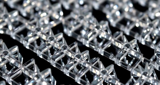
Crystals and grids are powerful tools often used to enhance energy work, meditation, and manifestation practices. But beyond their spiritual applications, they also play a crucial role in materials science and manufacturing, where their geometric properties influence performance and stability. Understanding lattice symmetry is essential when working with crystals, as it describes the repeating pattern of atoms that make up their structure. This symmetry determines how a crystal interacts with light, heat, and mechanical stress, making it critical for designing materials with specific properties. When you analyze lattice symmetry, you gain insight into a crystal’s internal architecture, which helps in selecting the right crystal for a particular application, whether it’s electronics, optics, or structural materials.
Understanding lattice symmetry reveals a crystal’s internal architecture, guiding material selection for electronics, optics, and structural applications.
Grid optimization becomes equally important when you use crystals in technological and manufacturing processes. By carefully arranging crystals and their internal lattices, you can maximize their efficiency and strength. This process involves fine-tuning the orientation and placement of crystals within a grid to guarantee uniform energy distribution, minimal defects, and enhanced performance. For instance, in semiconductor fabrication, aligning crystal lattices precisely can markedly improve electrical conductivity and device reliability. When you’re designing grids for energy transfer or structural support, understanding how to optimize the lattice symmetry allows you to create more durable and effective products.
In practical terms, grid optimization involves adjusting the geometry of how crystals are arranged and interact within a larger system. You might manipulate the angles, spacing, or orientation of individual crystals to achieve the desired outcome. This meticulous approach is essential in manufacturing processes like photovoltaic cells, where maximizing light absorption depends on the precise alignment of crystal lattices. Similarly, in the creation of advanced composites, the way crystals are organized within a matrix determines the material’s overall strength and flexibility. By harnessing the principles of lattice symmetry and grid optimization, you can engineer materials that meet exact specifications, improving both their functionality and longevity. Recognizing how the geometric properties of crystals influence their behavior allows engineers to push the boundaries of manufacturing and create solutions that are both advanced and sustainable.
Ultimately, whether you’re working on energy grids, electronic devices, or structural components, a deep understanding of crystal geometry and lattice symmetry empowers you to innovate and refine your designs. Mastering grid optimization guarantees that you utilize the inherent properties of crystals to their fullest potential, leading to stronger, more efficient, and more reliable materials. Recognizing how these geometric principles influence material behavior allows you to push the boundaries of manufacturing and create solutions that are both advanced and sustainable.
Frequently Asked Questions
How Do Crystal Defects Influence Material Properties?
Crystal defects markedly influence your material’s properties by disrupting dislocation dynamics and creating vacancy formations. These defects can weaken the material, making it more prone to deformation or failure under stress. Conversely, some defects can enhance properties like ductility or electrical conductivity. By controlling defect types and densities, you can tailor materials to meet specific application needs, improving durability and performance in various environments.
Can Grid Design Optimize Manufacturing Efficiency?
Yes, grid design can enhance manufacturing efficiency by improving grid optimization strategies. When you carefully plan the grid layout, you reduce material waste and streamline production processes, which boosts manufacturing throughput. Efficient grid patterns help guarantee materials are used effectively, machinery runs smoothly, and production time minimizes delays. By focusing on ideal grid design, you can markedly improve overall manufacturing performance and achieve better resource management.
What Role Does Symmetry Play in Crystal Stability?
Imagine a perfectly balanced dance where each move complements the next—that’s symmetry in crystals. It plays a vital role in stability by satisfying symmetry constraints, which allows atoms to fit together harmoniously. This alignment reduces energy, leading to energy minimization, making the crystal more stable. When symmetry is optimized, your crystal structure becomes resilient, less prone to defects, and more capable of withstanding environmental stresses.
Are There New Materials Emerging From Grid-Based Fabrication?
Yes, grid pattern innovations are driving the development of emerging material applications. You can explore new materials with tailored properties by manipulating these grid structures, which enable lightweight, strong, and flexible designs. Advances in fabrication techniques allow you to create complex, precise grid patterns that open doors to innovative uses in aerospace, biomedicine, and electronics. This evolution in grid-based fabrication continually pushes the boundaries of what materials can achieve.
How Do Environmental Factors Affect Crystal Growth?
Environmental factors can dramatically influence crystal growth—sometimes more than you’d think, like a storm shaping a mountain. You affect growth kinetics through temperature, pressure, and chemical environment, which in turn control crystal structure and quality. Fluctuations in environmental conditions can cause defects or alter growth rates, so precise control is vital for consistent results. You need to carefully manage these factors to optimize crystal development and ensure desired material properties.
Conclusion
As you explore crystals and grids, you realize how geometry shapes the materials around you—often in ways you don’t notice. Coincidentally, the same patterns that govern tiny structures also influence larger designs, connecting science and everyday life. It’s fascinating how these natural and manufactured grids mirror each other, revealing a hidden order. So, next time you see a crystal or a grid, remember—you’re witnessing the universe’s geometry in action, just waiting for you to discover it.